


I/O Expander
Flexibility is the main advantage of using an 8-bit MCU to build an I/O expander. The MCU which belongs to Embedded IC and a part of it can design its behavior based on the software it executes, whereas the I/O expander ASIC’s feature set is inherent in the device. Due to its adaptability, the MCU-based version can be customized to meet the requirements of the final application.
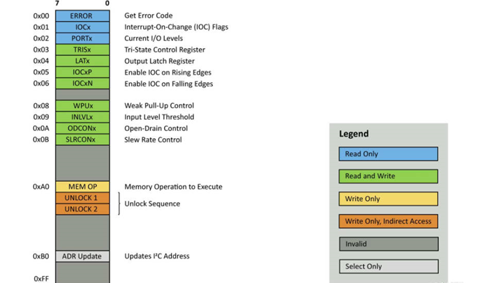
Implementing Advanced I/O Expander
The Advanced I/O Expander uses a lookup table-based internal architecture to function. A virtual address is sent before a read or write. This address is exclusive to the lookup table and not related to the MCU’s registers. This enables the seamless addition of functionality that is not present in the hardware registers of the MCU. For certain needs, the table’s entries can also be simply rearranged. The lookup table’s flexibility to accept additional permissions is another
advantage of this structure. As an illustration, simply omit the write lookup table item to construct a read-only register.
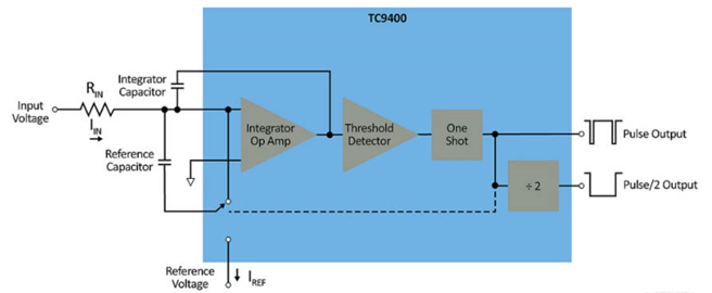
Voltage to Frequency (V/F) Converter
By lowering the bill of materials (BOM) and design area, V/F converters improve conventional analog systems. The majority of V/F converters on the market need external resistors and capacitors to function, whereas all MCUs simply need basic decoupling and pull-up components.
The MCU uses a combination of peripherals and functionalities that are independent of the core in place of analog technology for digitization. While a microprocessor only has a single central processing unit, a micro controller has a CPU, memory, and I/O all built into a single chip. While a microcontroller is useful in embedded systems, a microprocessor is beneficial in personal computers. The MCU measures the input signals with an inbuilt analog-to-digital converter with computation (ADCC), divides the clock signals, and outputs a variable-frequency signal. In this illustration, following initialization, the peripherals have been configured to operate independently of the CPU. This indicates that the final application can utilize the CPU for additional tasks.
The MCU-based technique has the drawback of not performing as well as analog alternatives. The ADCC has an inherent limit on the output resolution. Although the ADCC is nominally 12-bit, depending on how the application is set up, it actually operates at an oversampled 14-bit resolution. Similar to this, depending on the value determined by ADCC, the on-chip numerically controlled oscillator (NCO) that synthesizes the output frequency may have jitter in its output.
Output Oscillator Module
The output oscillator module of this solution is responsible for generating a clock signal at the desired output frequency. This output signal is internally connected to a duty cycle generator, which in turn halves the output frequency, but produces a 50% duty cycle output. Thus, the output oscillator module operates at twice the output frequency.
The heart of the output oscillator module is the NCO (Figure 6).The NCO peripheral operates by adding incremental values to the accumulator on the rising edge of the input clock. Accumulator overflow is used to obtain the output of the peripheral.
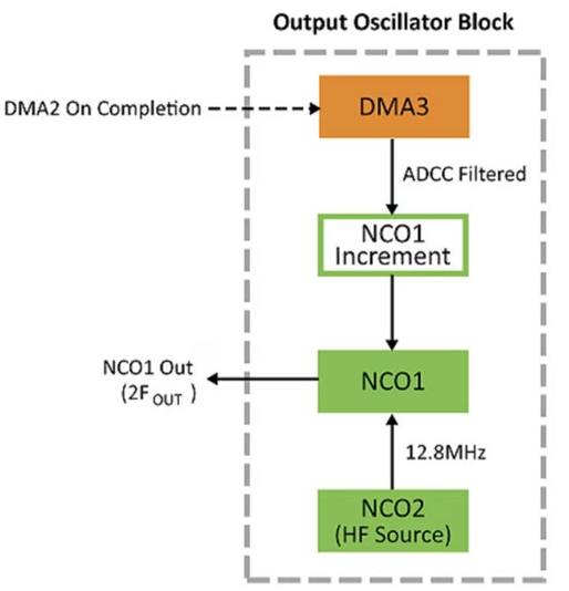
In this illustration, the NCO2 has been configured to provide the necessary input clock frequency internally in order to produce a 100 kHz output from a 14-bit input. The 12-bit result from the ADCC alone is insufficient to provide a 100kHz output without an additional clock source, so the 14-bit result is used instead. The output frequency will scale to a different output range if the NCO2’s output frequency is altered or if a different source is utilized. The output, for instance, will be no more than 10kHz if the NCO2 is scaled down to 1.28MHz.
Duty Cycle Generator
This feature is optional, and although the duty cycle will vary to a greater extent, the output of the NCO can be used directly. The generator is implemented using one of the Configurable Logic Cells (CLCs), which are small modules of discrete configurable logic similar to the individual cells of an FPGA.The CLCs can be used as discrete logic gates, such as AND-OR or OR-XOR.They can also be configured as latches or flip-flops. In this solution, the CLC is implemented as a JK flip-flop with reset. j and k are held at logic high. The output oscillator module is used as a clock for the flip-flop. Each input clock pulse causes the output to toggle, resulting in a 50% duty cycle. It is important to note that frequency jitter from the output oscillator module affects the duty cycle.
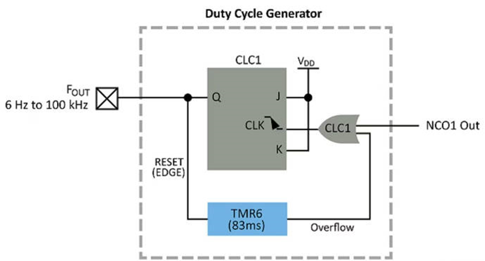
Timer 6 is employed as a “watchdog” timer that is insecure. The timer will overrun and produce a clock pulse for the CLC if the output does not cause an edge (rising or falling). The low end of the output frequency range is controlled by this. The output will transition at half the timer frequency, or 6Hz, rather than reaching DC.


