Introduction
Thin Film Transistors (TFTs) are a cornerstone technology in modern electronics, particularly in the realm of display technology and integrated circuits. They are essentially semiconductor devices that are fabricated by depositing thin films of various materials onto a substrate. The unique properties of TFTs, such as their ability to be manufactured on large-area substrates and their compatibility with various display technologies like Liquid Crystal Displays (LCDs) and Organic Light Emitting Diodes (OLEDs), have made them indispensable in the electronics industry.
Basic Structure and Working Principle
Structure
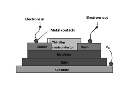
A typical TFT consists of several key components:
- Substrate: The base material on which the TFT is built. Common substrates include glass, plastic, and silicon.
- Semiconductor Layer: This is the active layer where the switching action occurs. It is usually made from materials like amorphous silicon (a-Si), polycrystalline silicon (poly-Si), or organic semiconductors.
- Source and Drain Electrodes: These are the terminals through which current flows into and out of the semiconductor layer.
- Gate Insulator: An insulating layer that separates the gate electrode from the semiconductor layer.
- Gate Electrode: This controls the flow of current between the source and drain by modulating the electric field in the semiconductor layer.
Working Principle
The operation of a TFT is based on the field-effect principle. When a voltage is applied to the gate electrode, an electric field is created across the gate insulator. This field can either attract or repel charge carriers (electrons or holes) in the semiconductor layer, thereby creating a conductive channel between the source and drain electrodes. The amount of current that flows between the source and drain is controlled by the voltage applied to the gate, making the TFT an excellent switch or amplifier.
Types of Thin Film Transistors
Amorphous Silicon (a-Si) TFTs
Amorphous silicon TFTs are the most widely used type in LCD displays. They are relatively easy to manufacture and can be produced on large-area substrates. However, their performance is limited by the relatively low mobility of charge carriers in amorphous silicon, which restricts their switching speed and current-carrying capacity.
Polycrystalline Silicon (poly-Si) TFTs
Poly-Si TFTs offer higher carrier mobility compared to a-Si TFTs, making them suitable for applications requiring higher performance, such as high-resolution displays and integrated circuits. The manufacturing process for poly-Si TFTs is more complex and expensive, involving techniques like laser annealing to crystallize the silicon.
Organic TFTs (OTFTs)
OTFTs use organic materials as the semiconductor layer. They have the potential for flexible and low-cost applications due to the ability to process these materials using solution-based techniques. However, their performance is still being improved to match that of inorganic TFTs.
Fabrication Techniques
Deposition Methods
Thin films in TFTs are typically deposited using techniques such as:
- Chemical Vapor Deposition (CVD): This involves the chemical reaction of gaseous precursors to form a solid film on the substrate. Plasma Enhanced CVD (PECVD) is a variant that uses a plasma to enhance the deposition process.
- Physical Vapor Deposition (PVD): This includes methods like sputtering and evaporation, where material is physically transferred from a source to the substrate.
- Spin Coating: Used primarily for organic materials, where a liquid precursor is spun onto the substrate and then dried to form a film.
Patterning Techniques
After deposition, the thin films need to be patterned to form the desired structures. This is typically done using photolithography, where a light-sensitive material (photoresist) is used to transfer a pattern from a mask to the substrate. The pattern is then etched into the film using wet or dry etching techniques.
Applications
Display Technology
TFTs are integral to modern display technologies:
- Liquid Crystal Displays (LCDs): a-Si TFTs are used to control the orientation of liquid crystal molecules, thereby modulating the amount of light that passes through each pixel.
- Organic Light Emitting Diode (OLED) Displays: Both a-Si and poly-Si TFTs are used in OLED displays to drive the organic light-emitting materials.
Integrated Circuits
TFTs are also used in large-area integrated circuits, where they can be used to create complex electronic circuits on substrates like glass or plastic. This has applications in smart packaging, RFID tags, and flexible electronics.
Challenges and Future Directions
Challenges
- Performance: Improving the carrier mobility and switching speed of TFTs is an ongoing challenge, especially for organic and amorphous silicon-based devices.
- Stability: Ensuring the long-term stability and reliability of TFTs, particularly in harsh environments, is crucial for their widespread adoption.
- Cost: Reducing the manufacturing cost of high-performance TFTs, especially poly-Si and OTFTs, is essential for their competitiveness.
Future Directions
- New Materials: Research into new semiconductor materials, such as metal oxides and 2D materials like graphene, holds promise for improving TFT performance.
- Flexible Electronics: The development of flexible and stretchable TFTs is a key area of research, with potential applications in wearable technology and flexible displays.
- High-Resolution Displays: As display technology advances, the demand for higher resolution and faster refresh rates will drive the development of more sophisticated TFT technologies.
Conclusion
Thin Film Transistors have revolutionized the electronics industry, particularly in the field of display technology. Their ability to be manufactured on large-area substrates and their compatibility with various display technologies make them a versatile and essential component. While there are challenges to be addressed, ongoing research and development are paving the way for even more advanced and versatile TFT technologies in the future.


